The used manufacturing technology guarantees highest reproducibility:
We fulfill most challenging series manufacturing demands for custom micro lens arrays with our advanced in-house toolmaking capabilities, years of expertise in glass molding, strict quality control, and continuous upgrading of optical measurement technologies in the micro-domain. That is why we can now introduce our 10×10 plano-convex microlens array developed as a technology demonstrator for the collimation of 2D fiber arrays in free-space, showcasing the many advantages of the technology and give R&D specialists an opportunity to test the MLAs live in optical assemblies.
The Sample Product:
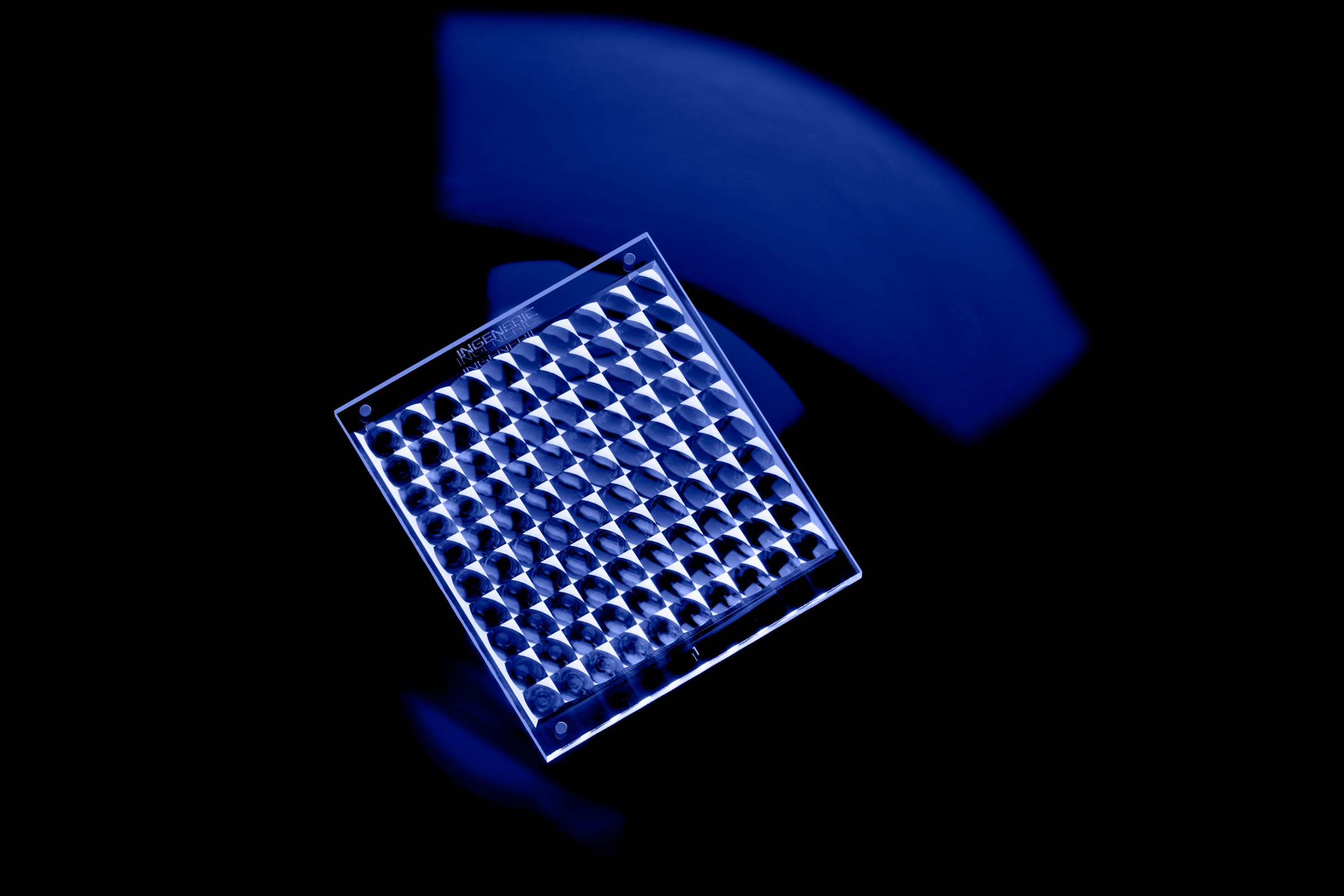
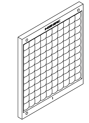
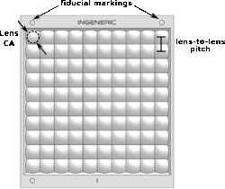 INGENERIC 2D Fiber Collimator Array 10×10 MLA
- Two-dimensional, plano-convex glass microlens array (10×10)
- Combination of fiber array and microlens array forms principal architecture of fiber collimator arrays for optical switches
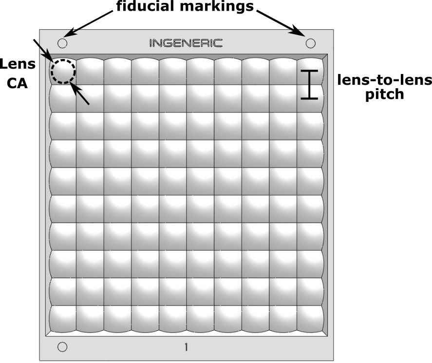
- Radius of curvature shows high design accuracy of the molding process. The mold form is repeatedly transferred on wafers.
- The low form errors ensure low wave-front aberrations on lenses so that highest transmission efficiencies and high MTFs (Modular Transfer Function) for imaging applications and low insertion losses for optical communication devices are achieved.
- During the in-house toolmaking process, engineering optimum toolpath kinematics allow master molds with highest surface finish. The reproducible mold-wafer feature transfer process allows low areal roughness (< 15 nm) on the glass surface to be achieved for applications at infra-red wavelengths.
- Highly precise master mold with sub-micron design accuracy is realized and pitch on the mold is carefully engineered so that minimum positional errors between neighboring lenses is achieved after molding.
- Advantage > Our 2D test arrays show an excellent agreement to nominal design parameters and achieves highest tolerances.
Advantages of the INGENERIC 2D MLA: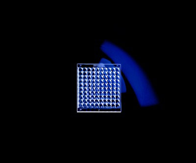
- Precision Molding:
- Process ensures stable and highly reproducible feature transfer from mold to glass.
- From mold to wafers:
- Wafers display high radius conformity, minimal form errors, and low roughness.
- Our MLA test sample
- fulfills tight tolerance requirements to achieve 90% coupling efficiencies.
- Lenses:
- small pitch errors between lenses make sure that beam-pointing errors for fiber-collimation applications are kept to minimum.
- Measurements
- show excellent agreement with the nominal design parameters.
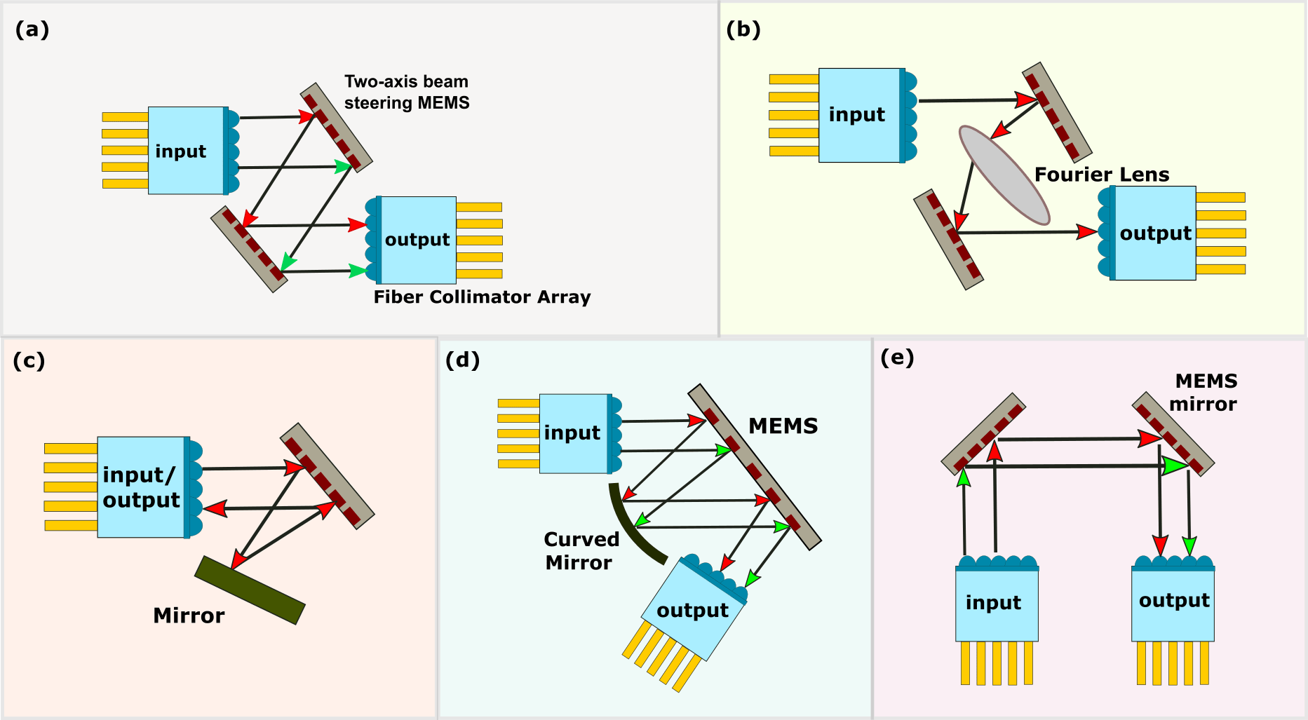
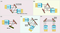
Free space 3D switching with MEMS optical cross-connects (OXCs)
 Typical Fields of Application:
- Datacenter Networking
- Core level switching to route signals between servers
- High Speed Telecom. Core Network
- Switching in reconfigurable mesh topology networks in combination with wavelength selective switching
- WDM-PON Networks
- Upgrade access networks with WDM over passive optical networks (PON)
Advantages:
- High scalable port count (e.g. 320×320)
- Ultrahigh bandwidth capacity (e.g. 32 Tbits)
- Millisecond scale switching speed (10-20ms)
- Low latency communication
You want to learn more about the INGENERIC MLAs for optical switching and talk to our experts about your project?
Description of typical procedure: From your RFQ to the customized product
From your RFQ to the final product there are usually several iterations to be made. A typical process is described below:
After having received your request, the next step is to review and maybe adapt your design with our technical engineering team to make it fit perfectly to our production technology. This may also include the choice of the best glass, the design of transition areas, etc. – always in close coordination with you, our customer.
With the final approval form your side, we can do the exact price calculations of item and NRE costs, i.e. for small and/or bigger molds. When having received your order, we can start to produce the tools and first prototypes. In general, no more adaptions are necessary then and we can continue our cooperation and scale up to volume production.